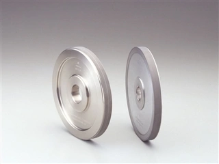
Diamond wheels for edge grinding (beveling) semiconductor wafers
This wheel is used for edge grinding (beveling) semiconductor wafers.
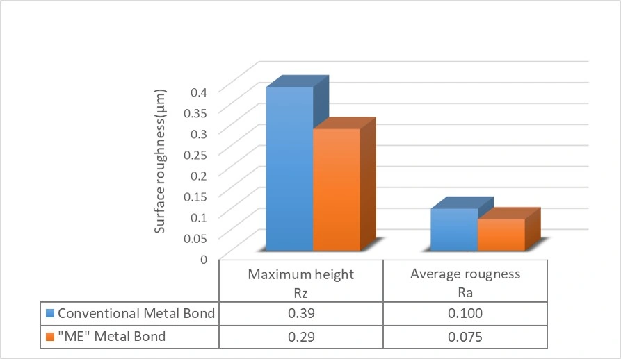
We offer “ME” bond for wheels for chamfering silicon wafers with excellent sharpness and high maintenance of groove shape. The finished surface roughness is excellent, and the amount of polishing after chamfering is reduced, leading to lower total processing costs by reducing the post-process time and consumables.
For wheels for chamfering SiC and sapphire wafers, we offer bond wheels with excellent sharpness and grinding durability. Electrodeposition bond chamfering wheels are also available for small and medium volume production.
For wheels for chamfering LT and LN wafers, we offer bond specifications that suppress the occurrence of chipping on brittle wafers.
In addition to general R-shaped (round/full round) and T-shaped grooves, special shapes such as asymmetrical shapes are also covered, so please consult with us.
[Applicable materials for diamond beveling wheels]
Silicon, SiC (silicon carbide), Sapphire, LT (lithium tantalate), LN (lithium niobate), GaN (gallium nitride), GaAs (gallium arsenide), and Quartz
Surface roughness comparison of grinding test of silicon wafer(after 120 pcs)
Reference sizes and specifications for diamond beveling wheels
- Grain size : #400 - #3000
- *It is possible to manufacture wheels usable for both roughing and finishing
- Outer diameter: φ102, φ202
- (Please contact us for other sizes.)
- Internal diameter tolerance: H6
- (Please consult with us for other tolerances.)
- Dynamic balance: ≥ 0.1 g @Min.
- Groove angle tolerance: Tolerance ≥ 0.5 degrees (one side angle)
Longer life of edge grinding (beveling) wheels for compound semiconductor wafers
[Issues in beveling compound semiconductor wafers]
The production of compound semiconductor wafers, which are used as substrates for power devices, is expected to grow steadily in the trend toward power saving in a low-carbon society. The key to this growth is the machining cost of wafers, and it is important to improve the life of diamond tools in the edge grinding (beveling) process. It is necessary to reduce chipping and extend the wheel life.
[Solution with metal bond beveling wheel]
A longer wheel life leads to benefits such as shorter cycle time with less replacement of tools and lower total cost of use. Our metal bond edge grinding (beveling) wheels are optimized for SiC (Silicon Carbide) and GaN (Gallium Nitride) wafer machining to reduce chipping and achieve long tool life.
We also offer electroplated edge grinding (beveling) wheels with excellent sharpness and cost performance.


Comparison of beveling wheel life for SiC wafers

Life improved by more than 30% compared to wheels made by other companies
By improving the geometric accuracy of the wheel and developing a metal bond optimized for compound semiconductor wafers, we were able to obtain the test result that the wheel life in the SiC wafer edge grinding (beveling) process increased by more than 30% compared to other manufacturers’ products.
Optimal grinding tools for beveling semiconductor wafers
Metal bond wheel for compound semiconductor wafers

[Possible production range]
Grain size : #400 – #3000 *Compound grain size is also available.
Outer diameter : Up to 202D
Internal diameter tolerance: H6
(Please consult with us for other tolerances.)
Dynamic balance: ≧0.1 g @Min.
Groove shape tolerance : ≧ 0.5 degrees
Number of grooves: Up to 10 grooves (more than 10 grooves are possible
depending on groove shape.)
- Diamond with unique abrasive grain control is used to reduce the incidence of chipping and the machining damage.
- The use of a bond with excellent abrasion resistance ensures high dimensional stability of the wheel shape and long life.